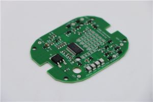
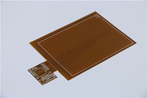
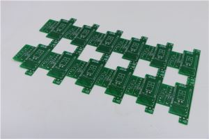
2 Layer Rigid Pcb For Communication With Surfacing Finished Is ENIG 1U''
Min.Order : 1 Pieces Quick Quotation >
Item Details
Product Description
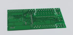
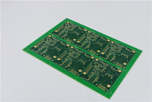
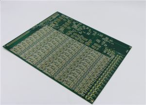
We supply multilayer gold plating rigid pcb thickness 1u''with Green solder mask rigid , PSPCB have been making pcb for more then 24years to overseas customer from USA,EU,Austrialia,New Zealand.
2 layer rigid pcb with surfacing finished is ENIG 1U''and customed 1 OZ copper finished for communication,usually made green solder mask and white silkscreen .
Rigid PCB Capability
Classification | Items | Capability | ||
Materials | Base-material | FR4, CEM-3, high frequency, PTFE, halogen-free , Aluminium base material, Copper based material | ||
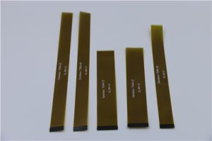
Material brand | KB, ITEQ, SY, ISOLA, Rogers, Arlon, Ventec, Laird, or other laminate on customer’s request. | |||
Min. core thickness | 3 mil | |||
Prepreg | 1080 , 2116 , 7628 , 7630 | |||
Copper foil | 1/4 oz ~6 oz | |||
Solder mask | Rongda,Taiyo,Nanya or other brand on customer’s request | |||
Hole | Min. drill size | 0.2mm | ||
Min laser drill size | 3mil | |||
Hole diameter tolerance | ±0.05mm | |||
Hole location tolerance | ±2mil | |||
PTH | Aspect/ratio | 12:01 | ||
Image transfer | min line width/space | 3/3 mil | ||
Finished copper thickness | 6 oz | |||
Layer to layer registration | 2 mil | |||
Etching | Line width/space tolerance | ±10% | ||
Solder Mask | Via plug | via size :0.2-0.8mm | ||
S/M registration | 1 mil | |||
solder dam width | 4 mil | |||
Finishing | HASL | YES | ||
HAL Lead Free | YES | |||
OSP finishing | YES | |||
Immersion Silver | YES | |||
Immersion Tin | YES | |||
Gold finger | YES | |||
Immersion gold | YES | |||
Product | Layer count | 1~20 layers | ||
Board thickness | 0.3 ~ 6 mm | |||
Board thickness tolerance | ± 5% | |||
max board size | 800*650mm | |||
min V-score residuals | 0.1 mm | |||
Bow & twist | =0.50% (max cap) | |||
Outline tolerance | ± 0.1mm | |||
Impedance control PCB | YES | |||
Blind and buried via PCB | YES(laser and mechanical drill) | |||
High frequency PCB | YES | |||
Selective hard gold PCB | YES | |||
Carbon ink PCB | YES | |||
Aluminium base PCB | YES | |||
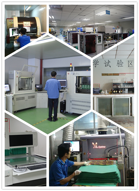
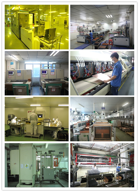
1. Below is our main production machine and inspection machine, our inspection machine have ON LINE AOI to check every single board after etching , Automatic E-test machine to check open and short circuitry, X-ray machine to check hole registration in inner layers. Two point measurement machine to check the size of the PCB. We have certificate of UL, ISO9001,ISO14000,ISO18001 and TS16949.
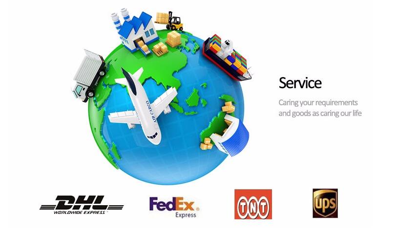
Shipping ways :TNT,UPS,FEDEX,DHL,BY SEA ,BY AIR ,BY TRAIN .
A:We respect customer’s copyright and will never manufacture PCB for someone else with your files unless we receive written.
permission from you, nor we’ll share these files with any other 3rd parties.
A: Yes,we could help you to clone the PCB. Just send the sample PCB to us, we could clone the PCB design and work out it.
Sample:
1-2 Layers: 5 to 7working days
4-8 Layers: 7-10 working days
Mass production:
1-2 Layers:7 to 15 working days
4-8 Layers:10 to 18 working days
The leadtime is depends on your final confirmed quantity.
A:-Wire Transfer(T/T)
B- Paypal
A:For small packages, we will ship the boards to you by DHL,UPS,FedEx,EMS. Door to door service! You will get your PCBs at your home.
For heavy goods more than 300kg, we may ship your PC boards by ship or by air to save freight cost.
Payment & Shipping

More Product
Recommend Product